
The 25th
European Microelectronics & Packaging Conference (EMPC 2025)
16 - 18 September 2025
World Trade Center, Grenoble | France
Keynote Speakers
Tuesday, 16/Sept/2025 – 9:10am – 9:55am
Propelling AI forward through Advanced Packaging Creativity
Ingu Yin Chang
Executive Vice President, ASE Inc.
Ingu Yin Chang is the Executive Vice President at ASE Inc., based in Sunnyvale, California. In his current role, he is responsible for developing and executing sales strategy, while driving global initiatives for ASE’s expanding packaging, systems, and integration solutions portfolio. Prior to joining ASE in 2013, Yin was CEO of Vertical Circuits Inc. (VCI), a company focused on the development of next generation vertical interconnect for next generation silicon integration. Previously, Yin performed a variety of management roles covering sales and operations at Amkor with responsibility for the Greater China region. He has over thirty years of leadership experience in executive management, sales, business development, IP management and strategic alliances. Yin received his material science engineering degree from University of California, Berkeley.
Abstract
The semiconductor industry is stacked with groundbreaking innovation that is helping to weave intelligence into every dimension of life, through generative, agentic and physical AI models, spanning all the way from the cloud to the edge. Heterogeneous Integration through advanced packaging is playing a pivotal role in pushing physical, electrical, and thermal limits to achieve better energy efficiency and greater compute power. During his keynote, ASE’s Yin Chang will set the stage by exploring the AI landscape, highlighting challenges that require our collective attention, particularly as we move from electrons to photons. He will then expand on how advanced packaging creativity is propelling AI forward by integrating higher-performance chips within smaller form factors for transformative latency improvement and bandwidth enhancement.
![YIN Chang 2025[64][53] Ingu Yin Chang<br />
Executive Vice President, ASE Inc.](https://empc2025.org/wp-content/uploads/2025/04/YIN-Chang-20256453.jpeg)
Ingu Yin Chang
Executive Vice President, ASE Inc.
Tuesday, 16/Sept/2025 – 9:55am – 10:40am
The Interconnect “Panelization”
Laurent Herard
Group VP – Head of Back End Manufacturing & Technology R&D, STMicroelectronics
Laurent Heard received an Engineering Degree in physics of semiconductor from the INP Grenoble France. He has thirty two years of experience in Packaging technology R&D and Back End assembly manufacturing in Europe, Morocco, Singapore and Malaysia. Laurent is a Company Fellow in the field of packaging and interconnect technology.
Abstract
The very fast innovation pace on AI processing hardware is pushing the semiconductor packaging industry to set up high volume production capability for ultra large very high-density interconnection interposers. This is creating a strong momentum for high density fan out Panel Level Packaging (PLP).
In the domain of electrification, there is a race to power density and efficiency. This is fueling the industry for designing and industrialize new ways to interconnect power chips with drivers and passives for low electrical losses, typically low RdsOn and low stray inductance.
Those two domains have very different requirements in terms of interconnect density and current capability, but they share the same technology trend with the integration of latest innovations from different interconnection manufacturing concepts: PCB, high density substrate, wafer level packaging, embedded die and passives, and traditional packaging technology such copper pillar flip chip, die attach sintering.
This presentation gives an overview of the Panel Level Packaging technology trends for main semiconductor applications. Then it presents the experience and key challenges faced during the industrialization of an actual high volume PLP manufacturing line.
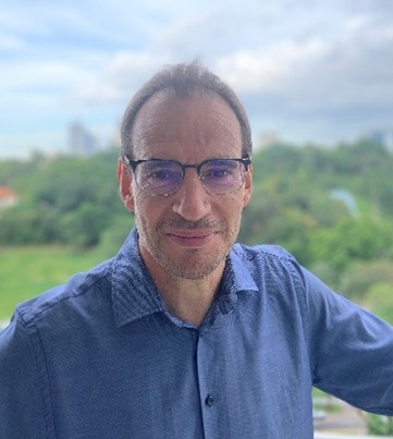
Laurent Herard
Group VP – Head of Back End Manufacturing & Technology R&D, STMicroelectronics
Tuesday, 16/Sept/2025 – 3:40pm – 4:25pm
Mass Transfer: How the Push for MicroLED Displays Opens New Paths to Heterogeneous Integration
Dr. Chris Bower
CTO and co-founder, X Display Company (XDC)., Inc.
Chris Bower is the Chief Technology Officer and co-founder of X Display Company (XDC). Before joining XDC, he was the Chief Technology Officer at X-Celeprint Limited, a company founded to develop and commercialize advanced micro assembly technologies. He was formerly a Technical Manager at Semprius, Inc., where he led the team responsible for elastomer-stamp mass transfer of silicon integrated circuits and compound semiconductor solar cells. His research interests include three-dimensional integration of integrated circuits, heterogeneous integration of compound semiconductors onto non-native substrates and the fabrication of low-cost, large-format electronics using novel assembly methods. He has co-authored over one hundred and thirty scientific publications and over one hundred and fifty patent applications.
Abstract
Assembling microLEDs into displays is challenging due to the need for precise placement of millions of tiny microLEDs. Fluidic self-assembly, laser transfer, and stamp transfer are all candidate technologies. Among these, elastomer stamp transfer has proven to be a scalable, high-yield solution. The advancements in mass transfer technology are now being applied to heterogeneous integration challenges beyond displays, enabling improved performance and flexibility in combining different types of components into complex electronic systems.

Dr. Chris Bower
CTO and co-founder, X Display Company (XDC)., Inc.
Wednesday, 17/Sept/2025 – 9:00am – 9:45am
Recent trends in automotive power module designs and technology for traction inverters
Dr. Uwe Hansen
VP Power Component Development, Bosch
Uwe Hansen received his PhD in Physics at the Technical University from Munich.
He specialized in theoretical semiconductor physics. Uwe started his career at Bosch as a process engineer in the Bosch automotive Waferfab, held various functions within Bosch related to semiconductors and was responsible for advanced packaging for CE and automotive MEMS. Since 2018 he is heading the department for power
component and module development at Bosch.
Abstract
In order to reduce the clearly visible trend of global warming, the changeover from fossil fuels to electrification is driven forward. Since transport largely contributes to C02 emissions the electrification of Plug-in Hybrid Electric Vehicles and Electric Vehicles is crucial. In this dynamic field power modules are needed that find the right balance between conflicting requirements like power density, scalability, design flexibility and performance. The challenge with modules in comparison to discretes is that part of the circuity is included in the module and that no standard is defined. In addition, due to the very different material and physical properties of wide band gap materials like SiC, learnings from the Si world can only be used to a limited extend. Emerging from the two different trends – frame based modules and molded modules – a concept combining the best of both and enabling 3D routing will be presented. The talk concludes with an outlook towards standardization due to the request for 2nd source capability.
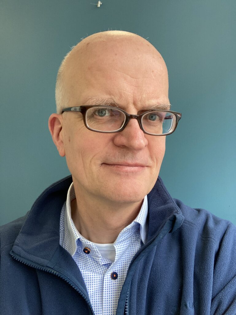
Dr. Uwe Hansen
VP Power Component Development, Bosch
Wednesday, 17/Sept/2025 – 9:45am – 10:30am
System Technology Co-optimization for Advanced 3D & Heterogeneous Integration
Sébastien Dauvé
CEO, CEA-Leti
Sébastien Dauvé was named CEO of CEA-Leti effective on July 1, 2021, after more than twenty years of experience in microelectronics technologies and their applications, including clean mobility, medicine of the future, cybersecurity, and power electronics.
Sébastien Dauvé started his career at the French Armament Electronics Center, where he worked on developing synthetic-aperture radar. In 2003, he joined CEA-Leti as an industrial transfer manager and supervised several joint research laboratories, in particular with the multinational Michelin.
In 2007, Sébastien Dauvé became a laboratory manager, then head of an R&D department in the area of sensors applied to the Internet of things and electric mobility. During this time, he supported the dissemination of new technologies in industry, including the automotive industry (Renault), aeronautics, national defense (SAFRAN), and microchips with the industry leader Intel. He played an active role in the creation of start-ups in application fields ranging from health to infrastructure security, leading to dozens of new jobs. In 2016, he became Director of the CEA-Leti Systems Division.
From sensors to wireless communication, Sébastien Dauvé has played an active role in the digital transformation, focused on coupling energy frugality and performance. He has made cross-disciplinary approaches central to innovation by harnessing the expertise of talented teams with diverse backgrounds. Their goal is to provide technological tools for meeting the major societal challenges of the future.
Sébastien Dauvé is a graduate of the French Ecole Polytechnique and the National Higher French Institute of Aeronautics and Space (ISAE-SUPAERO).
Abstract
The world’s digitalization is driving an enormous increase in data generation, expected to reach nearly 500 zettabytes by 2030. This data deluge leads to a dramatic rise in energy consumption, which is unsustainable in the medium term. Technological breakthroughs must be developed to significantly improve (by a factor of 1000) the power efficiency of electronics. Today, it is clear that a single technology cannot meet all the requirements of the most demanding computing and connectivity ICs. It is thus evident that heterogeneous 3D integration or advanced packaging is the way forward to combine different technologies and also enable novel architectures (such as chiplets) that bring various functions closer together. This talk will detail the different technologies under development, such as hybrid bonding, TSV (Through-Silicon Vias), interposers, and wafer-to-wafer or die-to-wafer approaches. Recent results and demonstrators will also be presented.
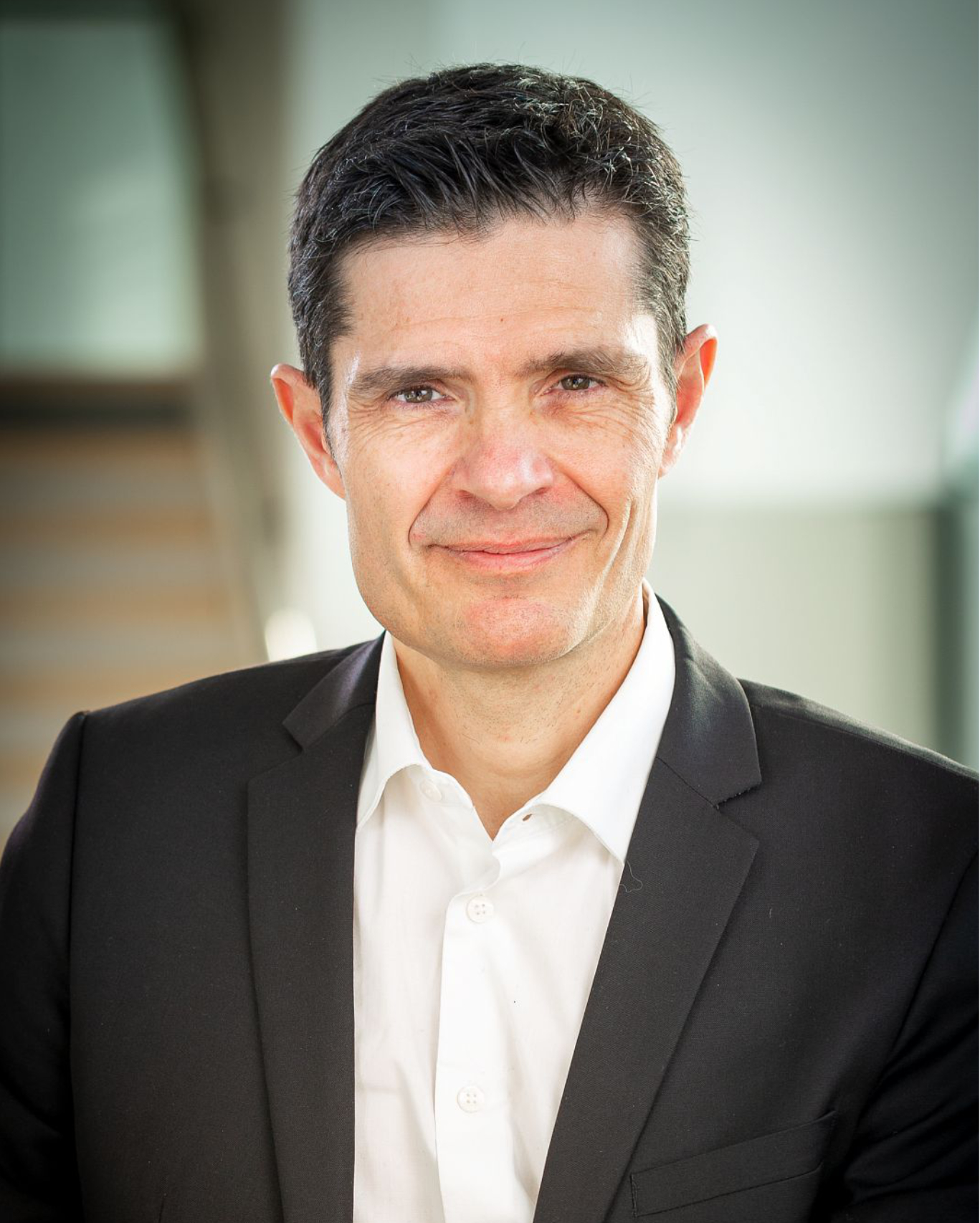
Sébastien Dauvé
CEO, CEA-Leti
Thursday, 18/Sept/2025 – 8:45am – 9:30am
Advanced Packaging – The Key Technology for Chiplet Integration
Prof. Dr.-Ing. Ulrike Ganesh
Managing Director, Fraunhofer IZM
Professor Ulrike Ganesh has over 21 years of experience in the semiconductor industry. She is Managing Director of Fraunhofer IZM (Institute for Reliability and Microintegration) and a professor at the Technical University of Berlin, where she holds the Chair of “Design and Hetero-Integration of Micro-Electronic Systems.” Throughout her career, she has worked with top companies including IBM, Qualcomm, and Bosch and research institutions in both Germany and the USA. Professor Ganesh earned her doctorate in electrical engineering from the Technical University of Berlin, specializing in failure analysis for semiconductor devices. Since her postdoctoral research, she has built and led teams focused on driving innovation. As head of Fraunhofer IZM, she is responsible for 450 experts in advanced semiconductor packaging. A passionate mentor, she actively supports the growth of young scientists and engineers. With her expertise in leadership, R&D, and strategic vision, she continues to shape the future of microelectronics.
Abstract
Chiplets are becoming key components: They not only help tackle the forces that are threatening to end Moore’s Law, they are also the crucial gateway technology for e.g. electro-optical systems, non-CMOS devices, and sensors, and they promise to sustain the race for high performance at low cost. Advanced packaging is key to the widespread acceptance of chiplets. With 30 years of experience in this field, Fraunhofer IZM plays a crucial role in the microelectronics community. The presentation will discuss the basics of chiplet integration and highlight their advantages over traditional monolithic chips. It addresses the challenges in terms of reliability and the associated design and development requirements and highlights the need to consider design optimization, material selection, test procedures, fault tolerance, and continuous improvement holistically and from the beginning. A combination of these is essential to make chiplet systems meaningfully more reliable.

Prof. Dr.-Ing. Ulrike Ganesh
Managing Director, Fraunhofer IZM
Thursday, 18/Sept/2025 – 2:00pm – 2:45pm
Charting a Path for the Chiplet Era and Beyond
Craig Bishop
Chief Technology Officer, Deca Technologies
Craig Bishop is Chief Technology Officer at Deca Technologies, managing the Adaptive Patterning technology, EDA development, intellectual property, and R&D. He is also Technical Director for the $100M SHIELD USA program in close collaboration with ASU to produce leap-ahead organic substrates under the National Advanced Packaging Manufacturing Program (NAPMP). Prior, Craig was the architect of Adaptive Patterning at Deca where he developed the technology and design methodologies that have been implemented in high-volume production, with over seven billion devices shipped in leading smartphones and other electronics. Craig Bishop received his B.S. degree in electrical and computer engineering from the University of Arizona in Tucson with specialization in analog IC design. He has over than two dozen patents issued related to fan-out and electronic interconnects.
Abstract
The chiplet era is upon our industry, driving exponentially increasing demand for die-to-die interconnect that is met with an expanding variety of package architectures. Interposers, hybrid bonding, and novel substrate technologies are approaching the scale of upper metals layers in a chip, driven by insatiable demand from artificial intelligence and high-performance computing applications. As electronic design automation tools catch up to these advancements, designers will completely blur the boundary between chip wires and package wires. Beyond these widely discussed applications, chiplets are coming for microcontrollers too, enabling the disaggregation of non-volatile memory, analog, and digital blocks. This talk will explore macro trends of the chiplet era and contemplate what path lies beyond – perhaps the monolithic decades will become a brief historical exception.

Craig Bishop
Chief Technology Officer, Deca Technologies